(from: https://www.desy.de/news/news_search/index_eng.html?openDirectAnchor=1939)
In the global race to measure ever shorter time spans, physicists from Goethe University Frankfurt have now taken the lead: together with colleagues at the accelerator facility DESY in Hamburg and the Fritz-Haber-Institute in Berlin, they have measured a process that lies within the realm of zeptoseconds for the first time: the propagation of light within a molecule. A zeptosecond is a trillionth of a billionth of a second (10-21 seconds).
Schematic representation of zeptosecond measurement. The photon (yellow, coming from the left) produces electron waves out of the electron cloud (grey) of the hydrogen molecule (red: nucleus), which interfere with each other (interference pattern: violet-white). The interference pattern is slightly skewed to the right, allowing the calculation of how long the photon required to get from one atom to the next. Photo: Sven Grundmann, Goethe University Frankfurt
In 1999, the Egyptian chemist Ahmed Zewail received the Nobel Prize for measuring the speed at which molecules change their shape. He founded femtochemistry using ultrashort laser flashes: the formation and breakup of chemical bonds occurs in the realm of femtoseconds. A femtosecond equals 0.000000000000001 seconds, or 10-15 seconds.
Now atomic physicists at Goethe University in Professor Reinhard Dörner’s team have for the first time studied a process that is shorter than femtoseconds by magnitudes. They measured how long it takes for a photon to cross a hydrogen molecule: about 247 zeptoseconds for the average bond length of the molecule. This is the shortest timespan that has been successfully measured to date.
The scientists carried out the time measurement on a hydrogen molecule (H2) which they irradiated with X-rays from the synchrotron lightsource PETRA III at the Hamburg accelerator centre DESY. The researchers set the energy of the X-rays so that one photon was sufficient to eject both electrons out of the hydrogen molecule.
Electrons behave like particles and waves simultaneously, and therefore the ejection of the first electron resulted in electron waves launched first in the one, and then in the second hydrogen molecule atom in quick succession, with the waves merging.
The photon behaved here much like a flat pebble that is skimmed twice across the water: when a wave trough meets a wave crest, the waves of the first and second water contact cancel each other, resulting in what is called an interference pattern.
The scientists measured the interference pattern of the first ejected electron using the COLTRIMS reaction microscope, an apparatus that Dörner helped develop and which makes ultrafast reaction processes in atoms and molecules visible. Simultaneously with the interference pattern, the COLTRIMS reactions microscope also allowed the determination of the orientation of the hydrogen molecule. The researchers here took advantage of the fact that the second electron also left the hydrogen molecule, so that the remaining hydrogen nuclei flew apart and were detected.
“Since we knew the spatial orientation of the hydrogen molecule, we used the interference of the two electron waves to precisely calculate when the photon reached the first and when it reached the second hydrogen atom,” explains Sven Grundmann whose doctoral dissertation forms the basis of the scientific article in Science. “And this is up to 247 zeptoseconds, depending on how far apart in the molecule the two atoms were from the perspective of light.”
Professor Reinhard Dörner adds: “We observed for the first time that the electron shell in a molecule does not react to light everywhere at the same time. The time delay occurs because information within the molecule only spreads at the speed of light. With this finding we have extended our COLTRIMS technology to another application.”
Publication: Sven Grundmann, Daniel Trabert, Kilian Fehre, Nico Strenger, Andreas Pier, Leon Kaiser, Max Kircher, Miriam Weller, Sebastian Eckart, Lothar Ph. H. Schmidt, Florian Trinter, Till Jahnke, Markus S. Schöffler, Reinhard Dörner: Zeptosecond Birth Time Delay in Molecular Photoionization. Science https://science.sciencemag.org/cgi/doi/10.1126/science.abb9318
Category Archives: Uncategorised
What are attoseconds? Nobel-winning physics explained
by Daniel Lawler and Juliette Collen (from phys.org)

The Nobel Physics Prize was awarded on Tuesday to three scientists for their work on attoseconds, which are almost unimaginably short periods of time.
Their work using lasers gives scientists a tool to observe and possibly even manipulate electrons, which could spur breakthroughs in fields such as electronics and chemistry, experts told AFP.
How fast are attoseconds?
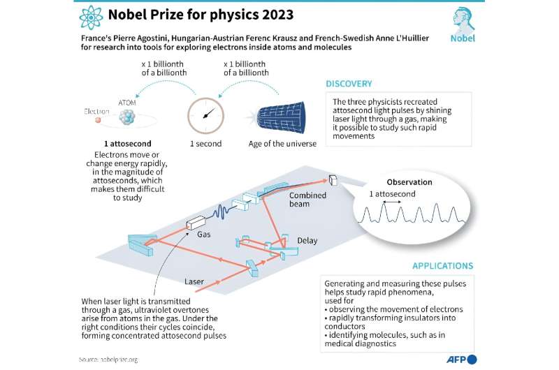
Attoseconds are a billionth of a billionth of a second.
To give a little perspective, there are around as many attoseconds in a single second as there have been seconds in the 13.8-billion year history of the universe.
Hans Jakob Woerner, a researcher at the Swiss university ETH Zurich, told AFP that attoseconds are “the shortest timescales we can measure directly”.
Why do we need such speed?
Being able to operate on this timescale is important because these are the speeds at which electrons—key parts of an atom—operate.
For example, it takes electrons 150 attoseconds to go around the nucleus of a hydrogen atom.
This means the study of attoseconds has given scientists access to a fundamental process that was previously out of reach.
All electronics are mediated by the motion of electrons—and the current “speed limit” is nanoseconds, Woerner said.
If microprocessors were switched to attoseconds, it could be possible to “process information a billion times faster,” he added.
How do you measure them?
Franco-Swede physicist Anne L’Huillier, one of the three new Nobel laureates, was the first to discover a tool to pry open the world of attoseconds.
It involves using high-powered lasers to produce pulses of light for incredibly short periods.
Franck Lepine, a researcher at France’s Institute of Light and Matter who has worked with L’Huillier, told AFP it was like “cinema created for electrons”.
He compared it to the work of pioneering French filmmakers the Lumiere brothers, “who cut up a scene by taking successive photos”.
John Tisch, a laser physics professor at Imperial College London, said that it was “like an incredibly fast, pulse-of-light device that we can then shine on materials to get information about their response on that timescale”.
How low can we go?
All three of Tuesday’s laureates at one point held the record for shortest pulse of light.
In 2001, French scientist Pierre Agostini’s team managed to flash a pulse that lasted just 250 attoseconds.
L’Huillier’s group beat that with 170 attoseconds in 2003.
In 2008, Hungarian-Austrian physicist Ferenc Krausz more than halved that number with an 80-attosecond pulse.
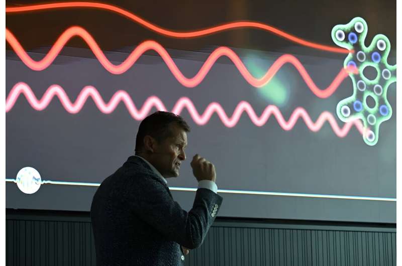
The current holder of the Guinness World Record for “shortest pulse of light” is Woerner’s team, with a time of 43 attoseconds.
The time could go as low as a few attoseconds using current technology, Woerner estimated. But he added that this would be pushing it.
What could the future hold?
Technology taking advantage of attoseconds has largely yet to enter the mainstream, but the future looks bright, the experts said.
So far, scientists have mostly only been able to use attoseconds to observe electrons.
“But what is basically untouched yet—or is just really beginning to be possible—is to control” the electrons, to manipulate their motion, Woerner said.
This could lead to far faster electronics as well as potentially spark a revolution in chemistry.
“We would not be limited to what molecules naturally do,” but instead could “tailor them according to need,” Woerner said.
So-called “attochemistry” could lead to more efficient solar cells, or even the use of light energy to produce clean fuels, he added.
Lightmatter’s Mars Chip Performs Neural-Network Calculations at the Speed of Light MIT spinoff harnesses optical computing to make neural-networks run faster and more efficiently
Milestone for compact particle accelerators, Laser trick produces high-energy terahertz pulses
From the colour difference of two slightly delayed laser flashes (left) a non-linear crystal generates an energetic terahertz pulse (from www.min.uni-hamburg.de/en/ )
A team of scientists from DESY and the University of Hamburg has achieved an important milestone in the quest for a new type of compact particle accelerator. Using ultra-powerful pulses of laser light, they were able to produce particularly high-energy flashes of radiation in the terahertz range having a sharply defined wavelength (colour). Terahertz radiation is to open the way for a new generation of compact particle accelerators that will find room on a lab bench. The team headed by Andreas Maier and Franz Kärtner from the Hamburg Center for Free-Electron Laser Science (CFEL) is presenting its findings in the journal Nature Communications. CFEL is jointly run by DESY, the University of Hamburg and the Max Planck Society.
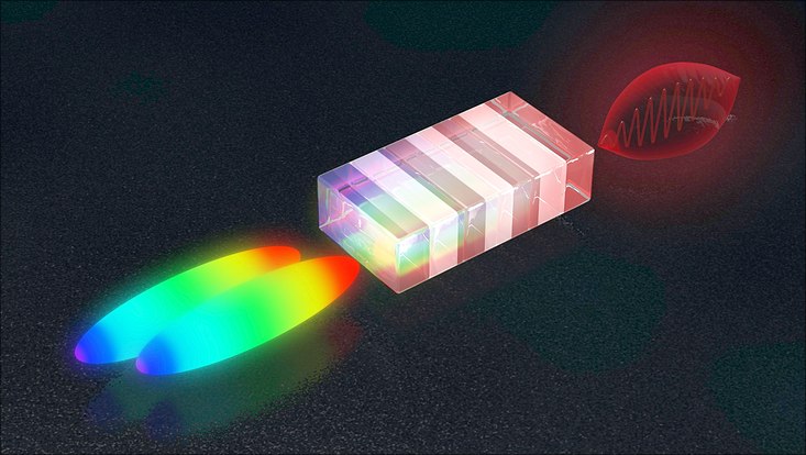
Photo: DESY/Lucid Berlin
The terahertz range of electromagnetic radiation lies between the infrared and microwave frequencies. Air travellers may be familiar with terahertz radiation from the full-body scanners used by airport security to search for objects hidden beneath a person’s garments. However, radiation in this frequency range might also be used to build compact particle accelerators. “The wavelength of terahertz radiation is about a thousand times shorter than the radio waves that are currently used to accelerate particles,” says Kärtner, who is a lead scientist at DESY. “This means that the components of the accelerator can also be built to be around a thousand times smaller.” The generation of high-energy terahertz pulses is therefore also an important step for the AXSIS (frontiers in Attosecond X-ray Science: Imaging and Spectroscopy) project at CFEL, funded by the European Research Council (ERC), which aims to open up completely new applications with compact terahertz particle accelerators.
However, chivvying (6/66: rushing) along an appreciable number of particles calls for powerful pulses of terahertz radiation having a sharply defined wavelength. This is precisely what the team has now managed to create. “In order to generate terahertz pulses, we fire two powerful pulses of laser light into a so-called non-linear crystal, with a minimal time delay between the two,” explains Maier from the University of Hamburg. The two laser pulses have a kind of colour gradient, meaning that the colour at the front of the pulse is different from that at the back. The slight time shift between the two pulses therefore leads to a slight difference in colour. “This difference lies precisely in the terahertz range,” says Maier. “The crystal converts the difference in colour into a terahertz pulse.”
The method requires the two laser pulses to be precisely synchronised. The scientists achieve this by splitting a single pulse into two parts and sending one of them on a short detour so that it is slightly delayed before the two pulses are eventually superimposed again. However, the colour gradient along the pulses is not constant, in other words the colour does not change uniformly along the length of the pulse. Instead, the colour changes slowly at first, and then more and more quickly, producing a curved outline. As a result, the colour difference between the two staggered pulses is not constant. The difference is only appropriate for producing terahertz radiation over a narrow stretch of the pulse.
“That was a big obstacle towards creating high-energy terahertz pulses,” as Maier reports. “Because straightening the colour gradient of the pulses, which would have been the obvious solution, is not easy to do in practice.” It was co-author Nicholas Matlis who came up with the crucial idea: he suggested that the colour profile of just one of the two partial pulses should be stretched slightly along the time axis. While this still does not alter the degree with which the colour changes along the pulse, the colour difference with respect to the other partial pulse now remains constant at all times. “The changes that need to be made to one of the pulses are minimal and surprisingly easy to achieve: all that was necessary was to insert a short length of a special glass into the beam,” reports Maier. “All of a sudden, the terahertz signal became stronger by a factor of 13.” In addition, the scientists used a particularly large non-linear crystal to produce the terahertz radiation, specially made for them by the Japanese Institute for Molecular Science in Okazaki.
“By combining these two measures, we were able to produce terahertz pulses with an energy of 0.6 millijoules, which is a record for this technique and more than ten times higher than any terahertz pulse of sharply defined wavelength that has previously been generated by optical means,” says Kärtner. “Our work demonstrates that it is possible to produce sufficiently powerful terahertz pulses with sharply defined wavelengths in order to operate compact particle accelerators.”
Original publication:
Spectral Phase Control of Interfering Chirped Pulses for High-Energy Narrowband Terahertz Generation,
S. W. Jolly, N. H. Matlis, F. Ahr, V. Leroux, T. Eichner, A.-L. Calendron, H. Ishizuki, T. Taira, F. X. Kärtner, and A. R. Maier,
Nature Communications 10, 2591 (2019).
MIT engineers develop “blackest black” material to date
MIT engineers report today that they have cooked up a material that is 10 times blacker than anything that has previously been reported. The material is made from vertically aligned carbon nanotubes, or CNTs — microscopic filaments of carbon, like a fuzzy forest of tiny trees, that the team grew on a surface of chlorine-etched aluminum foil. The foil captures at least 99.995 percent* of any incoming light, making it the blackest material on record. (from news.mit.edu)
The researchers have published their findings today in the journal ACS-Applied Materials and Interfaces. They are also showcasing the cloak-like material as part of a new exhibit today at the New York Stock Exchange, titled “The Redemption of Vanity.”
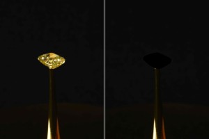
The artwork, a collaboration between Brian Wardle, professor of aeronautics and astronautics at MIT, and his group, and MIT Center for Art, Science, and Technology artist-in-residence Diemut Strebe, features a 16.78-carat natural yellow diamond from LJ West Diamonds, estimated to be worth $2 million, which the team coated with the new, ultrablack CNT material. The effect is arresting: The gem, normally brilliantly faceted, appears as a flat, black void.
 Wardle says the CNT material, aside from making an artistic statement, may also be of practical use, for instance in optical blinders that reduce unwanted glare, to help space telescopes spot orbiting exoplanets.
“There are optical and space science applications for very black materials, and of course, artists have been interested in black, going back well before the Renaissance,” Wardle says. “Our material is 10 times blacker than anything that’s ever been reported, but I think the blackest black is a constantly moving target. Someone will find a blacker material, and eventually we’ll understand all the underlying mechanisms, and will be able to properly engineer the ultimate black.”
Wardle’s co-author on the paper is former MIT postdoc Kehang Cui, now a professor at Shanghai Jiao Tong University.
Into the void
Wardle and Cui didn’t intend to engineer an ultrablack material. Instead, they were experimenting with ways to grow carbon nanotubes on electrically conducting materials such as aluminum, to boost their electrical and thermal properties.
But in attempting to grow CNTs on aluminum, Cui ran up against a barrier, literally: an ever-present layer of oxide that coats aluminum when it is exposed to air. This oxide layer acts as an insulator, blocking rather than conducting electricity and heat. As he cast about for ways to remove aluminum’s oxide layer, Cui found a solution in salt, or sodium chloride.
At the time, Wardle’s group was using salt and other pantry products, such as baking soda and detergent, to grow carbon nanotubes. In their tests with salt, Cui noticed that chloride ions were eating away at aluminum’s surface and dissolving its oxide layer.
“This etching process is common for many metals,” Cui says. “For instance, ships suffer from corrosion of chlorine-based ocean water. Now we’re using this process to our advantage.”
Cui found that if he soaked aluminum foil in saltwater, he could remove the oxide layer. He then transferred the foil to an oxygen-free environment to prevent reoxidation, and finally, placed the etched aluminum in an oven, where the group carried out techniques to grow carbon nanotubes via a process called chemical vapor deposition.
By removing the oxide layer, the researchers were able to grow carbon nanotubes on aluminum, at much lower temperatures than they otherwise would, by about 100 degrees Celsius. They also saw that the combination of CNTs on aluminum significantly enhanced the material’s thermal and electrical properties — a finding that they expected.
What surprised them was the material’s color.
“I remember noticing how black it was before growing carbon nanotubes on it, and then after growth, it looked even darker,” Cui recalls. “So I thought I should measure the optical reflectance of the sample.
“Our group does not usually focus on optical properties of materials, but this work was going on at the same time as our art-science collaborations with Diemut, so art influenced science in this case,” says Wardle.
Wardle and Cui, who have applied for a patent on the technology, are making the new CNT process freely available to any artist to use for a noncommercial art project.
“Built to take abuse”
Cui measured the amount of light reflected by the material, not just from directly overhead, but also from every other possible angle. The results showed that the material absorbed at least 99.995 percent of incoming light, from every angle. In other words, it reflected 10 times less light than all other superblack materials, including Vantablack. If the material contained bumps or ridges, or features of any kind, no matter what angle it was viewed from, these features would be invisible, obscured in a void of black.
The researchers aren’t entirely sure of the mechanism contributing to the material’s opacity, but they suspect that it may have something to do with the combination of etched aluminum, which is somewhat blackened, with the carbon nanotubes. Scientists believe that forests of carbon nanotubes can trap and convert most incoming light to heat, reflecting very little of it back out as light, thereby giving CNTs a particularly black shade.
“CNT forests of different varieties are known to be extremely black, but there is a lack of mechanistic understanding as to why this material is the blackest. That needs further study,” Wardle says.
The material is already gaining interest in the aerospace community. Astrophysicist and Nobel laureate John Mather, who was not involved in the research, is exploring the possibility of using Wardle’s material as the basis for a star shade — a massive black shade that would shield a space telescope from stray light.
“Optical instruments like cameras and telescopes have to get rid of unwanted glare, so you can see what you want to see,” Mather says. “Would you like to see an Earth orbiting another star? We need something very black. … And this black has to be tough to withstand a rocket launch. Old versions were fragile forests of fur, but these are more like pot scrubbers — built to take abuse.”
*An earlier version of this story stated that the new material captures more than 99.96 percent of incoming light. That number has been updated to be more precise; the material absorbs at least 99.995 of incoming light.
Kofi Annan
Kofi Atta Annan
8 April 1938 – 18 August 2018
was a Ghanaian diplomat who served as the seventh secretary-general of the United Nations from 1997 to 2006. Annan and the UN were the co-recipients of the 2001 Nobel Peace Prize. He was the founder and chairman of the Kofi Annan Foundation, as well as chairman of The Elders, an international organisation founded by Nelson Mandela.

