
(from: https://www.desy.de/news/news_search/index_eng.html?openDirectAnchor=1939)
In the global race to measure ever shorter time spans, physicists from Goethe University Frankfurt have now taken the lead: together with colleagues at the accelerator facility DESY in Hamburg and the Fritz-Haber-Institute in Berlin, they have measured a process that lies within the realm of zeptoseconds for the first time: the propagation of light within a molecule. A zeptosecond is a trillionth of a billionth of a second (10-21 seconds).
Schematic representation of zeptosecond measurement. The photon (yellow, coming from the left) produces electron waves out of the electron cloud (grey) of the hydrogen molecule (red: nucleus), which interfere with each other (interference pattern: violet-white). The interference pattern is slightly skewed to the right, allowing the calculation of how long the photon required to get from one atom to the next. Photo: Sven Grundmann, Goethe University Frankfurt
In 1999, the Egyptian chemist Ahmed Zewail received the Nobel Prize for measuring the speed at which molecules change their shape. He founded femtochemistry using ultrashort laser flashes: the formation and breakup of chemical bonds occurs in the realm of femtoseconds. A femtosecond equals 0.000000000000001 seconds, or 10-15 seconds.
Now atomic physicists at Goethe University in Professor Reinhard Dörner’s team have for the first time studied a process that is shorter than femtoseconds by magnitudes. They measured how long it takes for a photon to cross a hydrogen molecule: about 247 zeptoseconds for the average bond length of the molecule. This is the shortest timespan that has been successfully measured to date.
The scientists carried out the time measurement on a hydrogen molecule (H2) which they irradiated with X-rays from the synchrotron lightsource PETRA III at the Hamburg accelerator centre DESY. The researchers set the energy of the X-rays so that one photon was sufficient to eject both electrons out of the hydrogen molecule.
Electrons behave like particles and waves simultaneously, and therefore the ejection of the first electron resulted in electron waves launched first in the one, and then in the second hydrogen molecule atom in quick succession, with the waves merging.
The photon behaved here much like a flat pebble that is skimmed twice across the water: when a wave trough meets a wave crest, the waves of the first and second water contact cancel each other, resulting in what is called an interference pattern.
The scientists measured the interference pattern of the first ejected electron using the COLTRIMS reaction microscope, an apparatus that Dörner helped develop and which makes ultrafast reaction processes in atoms and molecules visible. Simultaneously with the interference pattern, the COLTRIMS reactions microscope also allowed the determination of the orientation of the hydrogen molecule. The researchers here took advantage of the fact that the second electron also left the hydrogen molecule, so that the remaining hydrogen nuclei flew apart and were detected.
“Since we knew the spatial orientation of the hydrogen molecule, we used the interference of the two electron waves to precisely calculate when the photon reached the first and when it reached the second hydrogen atom,” explains Sven Grundmann whose doctoral dissertation forms the basis of the scientific article in Science. “And this is up to 247 zeptoseconds, depending on how far apart in the molecule the two atoms were from the perspective of light.”
Professor Reinhard Dörner adds: “We observed for the first time that the electron shell in a molecule does not react to light everywhere at the same time. The time delay occurs because information within the molecule only spreads at the speed of light. With this finding we have extended our COLTRIMS technology to another application.”
Publication: Sven Grundmann, Daniel Trabert, Kilian Fehre, Nico Strenger, Andreas Pier, Leon Kaiser, Max Kircher, Miriam Weller, Sebastian Eckart, Lothar Ph. H. Schmidt, Florian Trinter, Till Jahnke, Markus S. Schöffler, Reinhard Dörner: Zeptosecond Birth Time Delay in Molecular Photoionization. Science https://science.sciencemag.org/cgi/doi/10.1126/science.abb9318
Author Archives: plug_the_plugger
Bandgap engineering of two-dimensional semiconductor materials (from nature.com)
A. Chaves, J. G. Azadani, Hussain Alsalman, D. R. da Costa, R. Frisenda, A. J. Chaves, Seung Hyun Song, Y. D. Kim, Daowei He, Jiadong Zhou, A. Castellanos-Gomez, F. M. Peeters, Zheng Liu, C. L. Hinkle, Sang-Hyun Oh, Peide D. Ye, Steven J. Koester, Young Hee Lee, Ph. Avouris, Xinran Wang & Tony Low
npj 2D Materials and Applications volume 4, Article number: 29 (2020)
Abstract
Semiconductors are the basis of many vital technologies such as electronics, computing, communications, optoelectronics, and sensing. Modern semiconductor technology can trace its origins to the invention of the point contact transistor in 1947. This demonstration paved the way for the development of discrete and integrated semiconductor devices and circuits that has helped to build a modern society where semiconductors are ubiquitous components of everyday life. A key property that determines the semiconductor electrical and optical properties is the bandgap. Beyond graphene, recently discovered two-dimensional (2D) materials possess semiconducting bandgaps ranging from the terahertz and mid-infrared in bilayer graphene and black phosphorus, visible in transition metal dichalcogenide, to the ultraviolet in hexagonal boron nitride. In particular, these 2D materials were demonstrated to exhibit highly tunable bandgaps, achieved via the control of layers number, heterostructuring, strain engineering, chemical doping, alloying, intercalation, substrate engineering, as well as an external electric field. We provide a review of the basic physical principles of these various techniques on the engineering of quasi-particle and optical bandgaps, their bandgap tuneability, potentials and limitations in practical realization in future 2D device technologies.
What are attoseconds? Nobel-winning physics explained
by Daniel Lawler and Juliette Collen (from phys.org)

The Nobel Physics Prize was awarded on Tuesday to three scientists for their work on attoseconds, which are almost unimaginably short periods of time.
Their work using lasers gives scientists a tool to observe and possibly even manipulate electrons, which could spur breakthroughs in fields such as electronics and chemistry, experts told AFP.
How fast are attoseconds?
Attoseconds are a billionth of a billionth of a second.
To give a little perspective, there are around as many attoseconds in a single second as there have been seconds in the 13.8-billion year history of the universe.
Hans Jakob Woerner, a researcher at the Swiss university ETH Zurich, told AFP that attoseconds are “the shortest timescales we can measure directly”.
Why do we need such speed?
Being able to operate on this timescale is important because these are the speeds at which electrons—key parts of an atom—operate.
For example, it takes electrons 150 attoseconds to go around the nucleus of a hydrogen atom.
This means the study of attoseconds has given scientists access to a fundamental process that was previously out of reach.
All electronics are mediated by the motion of electrons—and the current “speed limit” is nanoseconds, Woerner said.
If microprocessors were switched to attoseconds, it could be possible to “process information a billion times faster,” he added.

How do you measure them?
Franco-Swede physicist Anne L’Huillier, one of the three new Nobel laureates, was the first to discover a tool to pry open the world of attoseconds.
It involves using high-powered lasers to produce pulses of light for incredibly short periods.
Franck Lepine, a researcher at France’s Institute of Light and Matter who has worked with L’Huillier, told AFP it was like “cinema created for electrons”.
He compared it to the work of pioneering French filmmakers the Lumiere brothers, “who cut up a scene by taking successive photos”.
John Tisch, a laser physics professor at Imperial College London, said that it was “like an incredibly fast, pulse-of-light device that we can then shine on materials to get information about their response on that timescale”.
How low can we go?
All three of Tuesday’s laureates at one point held the record for shortest pulse of light.
In 2001, French scientist Pierre Agostini’s team managed to flash a pulse that lasted just 250 attoseconds.
L’Huillier’s group beat that with 170 attoseconds in 2003.
In 2008, Hungarian-Austrian physicist Ferenc Krausz more than halved that number with an 80-attosecond pulse.

The current holder of the Guinness World Record for “shortest pulse of light” is Woerner’s team, with a time of 43 attoseconds.
The time could go as low as a few attoseconds using current technology, Woerner estimated. But he added that this would be pushing it.
What could the future hold?
Technology taking advantage of attoseconds has largely yet to enter the mainstream, but the future looks bright, the experts said.
So far, scientists have mostly only been able to use attoseconds to observe electrons.
“But what is basically untouched yet—or is just really beginning to be possible—is to control” the electrons, to manipulate their motion, Woerner said.
This could lead to far faster electronics as well as potentially spark a revolution in chemistry.
“We would not be limited to what molecules naturally do,” but instead could “tailor them according to need,” Woerner said.
So-called “attochemistry” could lead to more efficient solar cells, or even the use of light energy to produce clean fuels, he added.
Lightmatter’s Mars Chip Performs Neural-Network Calculations at the Speed of Light MIT spinoff harnesses optical computing to make neural-networks run faster and more efficiently
Reply
Milestone for compact particle accelerators, Laser trick produces high-energy terahertz pulses
From the colour difference of two slightly delayed laser flashes (left) a non-linear crystal generates an energetic terahertz pulse (from www.min.uni-hamburg.de/en/ )
A team of scientists from DESY and the University of Hamburg has achieved an important milestone in the quest for a new type of compact particle accelerator. Using ultra-powerful pulses of laser light, they were able to produce particularly high-energy flashes of radiation in the terahertz range having a sharply defined wavelength (colour). Terahertz radiation is to open the way for a new generation of compact particle accelerators that will find room on a lab bench. The team headed by Andreas Maier and Franz Kärtner from the Hamburg Center for Free-Electron Laser Science (CFEL) is presenting its findings in the journal Nature Communications. CFEL is jointly run by DESY, the University of Hamburg and the Max Planck Society.
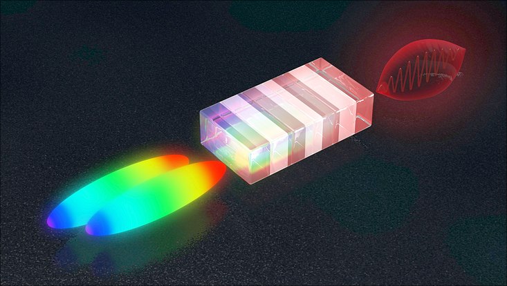
Photo: DESY/Lucid Berlin
The terahertz range of electromagnetic radiation lies between the infrared and microwave frequencies. Air travellers may be familiar with terahertz radiation from the full-body scanners used by airport security to search for objects hidden beneath a person’s garments. However, radiation in this frequency range might also be used to build compact particle accelerators. “The wavelength of terahertz radiation is about a thousand times shorter than the radio waves that are currently used to accelerate particles,” says Kärtner, who is a lead scientist at DESY. “This means that the components of the accelerator can also be built to be around a thousand times smaller.” The generation of high-energy terahertz pulses is therefore also an important step for the AXSIS (frontiers in Attosecond X-ray Science: Imaging and Spectroscopy) project at CFEL, funded by the European Research Council (ERC), which aims to open up completely new applications with compact terahertz particle accelerators.
However, chivvying (6/66: rushing) along an appreciable number of particles calls for powerful pulses of terahertz radiation having a sharply defined wavelength. This is precisely what the team has now managed to create. “In order to generate terahertz pulses, we fire two powerful pulses of laser light into a so-called non-linear crystal, with a minimal time delay between the two,” explains Maier from the University of Hamburg. The two laser pulses have a kind of colour gradient, meaning that the colour at the front of the pulse is different from that at the back. The slight time shift between the two pulses therefore leads to a slight difference in colour. “This difference lies precisely in the terahertz range,” says Maier. “The crystal converts the difference in colour into a terahertz pulse.”
The method requires the two laser pulses to be precisely synchronised. The scientists achieve this by splitting a single pulse into two parts and sending one of them on a short detour so that it is slightly delayed before the two pulses are eventually superimposed again. However, the colour gradient along the pulses is not constant, in other words the colour does not change uniformly along the length of the pulse. Instead, the colour changes slowly at first, and then more and more quickly, producing a curved outline. As a result, the colour difference between the two staggered pulses is not constant. The difference is only appropriate for producing terahertz radiation over a narrow stretch of the pulse.
“That was a big obstacle towards creating high-energy terahertz pulses,” as Maier reports. “Because straightening the colour gradient of the pulses, which would have been the obvious solution, is not easy to do in practice.” It was co-author Nicholas Matlis who came up with the crucial idea: he suggested that the colour profile of just one of the two partial pulses should be stretched slightly along the time axis. While this still does not alter the degree with which the colour changes along the pulse, the colour difference with respect to the other partial pulse now remains constant at all times. “The changes that need to be made to one of the pulses are minimal and surprisingly easy to achieve: all that was necessary was to insert a short length of a special glass into the beam,” reports Maier. “All of a sudden, the terahertz signal became stronger by a factor of 13.” In addition, the scientists used a particularly large non-linear crystal to produce the terahertz radiation, specially made for them by the Japanese Institute for Molecular Science in Okazaki.
“By combining these two measures, we were able to produce terahertz pulses with an energy of 0.6 millijoules, which is a record for this technique and more than ten times higher than any terahertz pulse of sharply defined wavelength that has previously been generated by optical means,” says Kärtner. “Our work demonstrates that it is possible to produce sufficiently powerful terahertz pulses with sharply defined wavelengths in order to operate compact particle accelerators.”
Original publication:
Spectral Phase Control of Interfering Chirped Pulses for High-Energy Narrowband Terahertz Generation,
S. W. Jolly, N. H. Matlis, F. Ahr, V. Leroux, T. Eichner, A.-L. Calendron, H. Ishizuki, T. Taira, F. X. Kärtner, and A. R. Maier,
Nature Communications 10, 2591 (2019).
Surprise graphene discovery could unlock secrets of superconductivity
Physicists make misaligned sheets of the carbon material conduct electricity without resistance. A sandwich of two graphene layers can conduct electrons without resistance if they are twisted at a ‘magic angle’, physicists have discovered. The finding could prove to be a significant step in the decades-long search for room-temperature superconductors. (from nature.com )
Most superconductors work only at temperatures close to absolute zero. Even ‘high-temperature’ superconductors are called that only in a relative sense: the highest temperature at which they conduct electricity without resistance is around −140 ºC. A material that displayed the property at room temperature — eliminating the need for expensive cooling — could revolutionize energy transmission, medical scanners and transport.
Physicists now report that arranging two layers of atom-thick graphene so that the pattern of their carbon atoms is offset by an angle of 1.1º makes the material a superconductor. And although the system still needed to be cooled to 1.7 degrees above absolute zero, the results suggest that it may conduct electricity much like known high-temperature superconductors — and that has physicists excited. The findings are published in two Nature papers1,2 on 5 March.
If confirmed, this discovery could be “very important” to the understanding of high-temperature superconductivity, says Elena Bascones, a physicist at the Institute of Materials Science of Madrid. “We can expect a frenzy of experimental activity over the next few months to fill in the missing parts of the picture,” says Robert Laughlin, a physicist and Nobel laureate at Stanford University in California.
Superconductors come broadly in two types: conventional, in which the activity can be explained by the mainstream theory of superconductivity, and unconventional, where it can’t. The latest studies suggest that graphene’s superconducting behaviour is unconventional — and has parallels with activity seen in other unconventional superconductors called cuprates. These complex copper oxides have been known to conduct electricity at up to 133 degrees above absolute zero. And although physicists have focused on cuprates for three decades in their search for room-temperature superconductors, the underlying mechanism has baffled them.
In contrast to cuprates, the stacked graphene system is relatively simple and the material is well-understood. “The stunning implication is that cuprate superconductivity was something simple all along. It was just hard to calculate properly,” says Laughlin.
Magic trick
Graphene already has impressive properties: its sheets, made of single layers of carbon atoms arranged in hexagons, are stronger than steel and conduct electricity better than copper. It has shown superconductivity before3, but it occurred when in contact with other materials, and the behaviour could be explained by conventional superconductivity.
Physicist Pablo Jarillo-Herrero at the Massachusetts Institute of Technology (MIT) in Cambridge and his team weren’t looking for superconductivity when they set up their experiment. Instead, they were exploring how the orientation dubbed the magic angle might affect graphene. Theorists have predicted that offsetting the atoms between layers of 2D materials at this particular angle might induce the electrons that zip through the sheets to interact in interesting ways — although they didn’t know exactly how.
The team immediately saw unexpected behaviour in their two-sheet set-up. First, measurements of graphene’s conductivity and the density of the particles that carry charge inside it suggested that the construction had become a Mott insulator2 — a material that has all the ingredients to conduct electrons, but in which interactions between the particles stop them from flowing. Next, the researchers applied a small electric field to feed just a few extra charge carriers into the system, and it became a superconductor1. The finding held up in experiment after experiment, says Jarillo-Herrero. “We have produced all of this in different devices and measured it with collaborators. This is something in which we’re very confident,” he says.
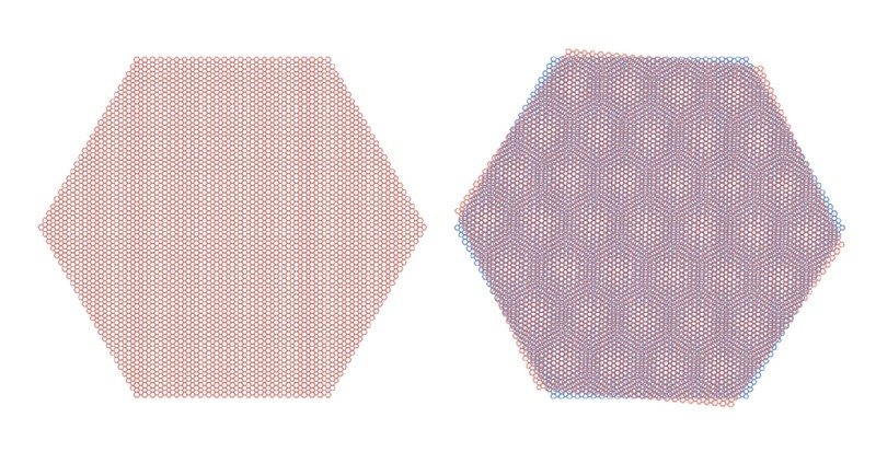
A material made up of two layers of graphene, twisted at an angle of 1.1º (illustrated, right), show superconducting properties.Courtesy of the researchers
The existence of an insulating state so close to superconductivity is a hallmark of unconventional superconductors such as cuprates. When the researchers plotted phase diagrams that charted the material’s electron density against its temperature, they saw patterns very similar to those seen for cuprates. That provides further evidence that the materials may share a superconducting mechanism, says Jarillo-Herrero.
Finally, although graphene shows superconductivity at a very low temperature, it does so with just one-ten-thousandth of the electron density of conventional superconductors that gain the ability at the same temperature. In conventional superconductors, the phenomenon is thought to arise when vibrations allow electrons to form pairs, which stabilize their path and allow them to flow without resistance. But with so few available electrons in graphene, the fact that they can somehow pair up suggests that the interaction at play in this system should be much stronger than what happens in conventional superconductors.
Conductivity confusion
Physicists disagree wildly on how electrons might interact in unconventional superconductors. “One of the bottlenecks of high-temperature superconductivity has been the fact that we don’t understand, even now, what’s really gluing the electrons into pairs,” says Robinson.
But graphene-based devices will be easier to study than cuprates, which makes them useful platforms for exploring superconductivity, says Bascones. For example, to explore the root of superconductivity in cuprates, physicists often need to subject the materials to extreme magnetic fields. And ‘tuning’ them to explore their different behaviours means growing and studying reams of different samples; with graphene, physicists can achieve the same results by simply tweaking an electric field.
Kamran Behnia, a physicist at the Higher Institute of Industrial Physics and Chemistry in Paris, is not yet convinced that the MIT team can definitively claim to have seen the Mott insulator state, although he says the findings do suggest that graphene is a superconductor, and potentially an unusual one.
Physicists cannot yet state with certainty that the superconducting mechanism in the two materials is the same. And Laughlin adds that it is not yet clear that all the behaviour seen in cuprates is happening in graphene. “But enough of the behaviours are present in these new experiments to give cause for cautious celebration,” he says.
Physicists have been “stumbling around in the dark for 30 years” trying to understand cuprates, says Laughlin. “Many of us think that a light just switched on.”