A. Chaves, J. G. Azadani, Hussain Alsalman, D. R. da Costa, R. Frisenda, A. J. Chaves, Seung Hyun Song, Y. D. Kim, Daowei He, Jiadong Zhou, A. Castellanos-Gomez, F. M. Peeters, Zheng Liu, C. L. Hinkle, Sang-Hyun Oh, Peide D. Ye, Steven J. Koester, Young Hee Lee, Ph. Avouris, Xinran Wang & Tony Low
npj 2D Materials and Applicationsvolume 4, Article number: 29 (2020)
Abstract
Semiconductors are the basis of many vital technologies such as electronics, computing, communications, optoelectronics, and sensing. Modern semiconductor technology can trace its origins to the invention of the point contact transistor in 1947. This demonstration paved the way for the development of discrete and integrated semiconductor devices and circuits that has helped to build a modern society where semiconductors are ubiquitous components of everyday life. A key property that determines the semiconductor electrical and optical properties is the bandgap. Beyond graphene, recently discovered two-dimensional (2D) materials possess semiconducting bandgaps ranging from the terahertz and mid-infrared in bilayer graphene and black phosphorus, visible in transition metal dichalcogenide, to the ultraviolet in hexagonal boron nitride. In particular, these 2D materials were demonstrated to exhibit highly tunable bandgaps, achieved via the control of layers number, heterostructuring, strain engineering, chemical doping, alloying, intercalation, substrate engineering, as well as an external electric field. We provide a review of the basic physical principles of these various techniques on the engineering of quasi-particle and optical bandgaps, their bandgap tuneability, potentials and limitations in practical realization in future 2D device technologies.
Physicists make misaligned sheets of the carbon material conduct electricity without resistance. A sandwich of two graphene layers can conduct electrons without resistance if they are twisted at a ‘magic angle’, physicists have discovered. The finding could prove to be a significant step in the decades-long search for room-temperature superconductors. (from nature.com )
Most superconductors work only at temperatures close to absolute zero. Even ‘high-temperature’ superconductors are called that only in a relative sense: the highest temperature at which they conduct electricity without resistance is around −140 ºC. A material that displayed the property at room temperature — eliminating the need for expensive cooling — could revolutionize energy transmission, medical scanners and transport.
Physicists now report that arranging two layers of atom-thick graphene so that the pattern of their carbon atoms is offset by an angle of 1.1º makes the material a superconductor. And although the system still needed to be cooled to 1.7 degrees above absolute zero, the results suggest that it may conduct electricity much like known high-temperature superconductors — and that has physicists excited. The findings are published in two Nature papers1,2 on 5 March.
If confirmed, this discovery could be “very important” to the understanding of high-temperature superconductivity, says Elena Bascones, a physicist at the Institute of Materials Science of Madrid. “We can expect a frenzy of experimental activity over the next few months to fill in the missing parts of the picture,” says Robert Laughlin, a physicist and Nobel laureate at Stanford University in California.
Superconductors come broadly in two types: conventional, in which the activity can be explained by the mainstream theory of superconductivity, and unconventional, where it can’t. The latest studies suggest that graphene’s superconducting behaviour is unconventional — and has parallels with activity seen in other unconventional superconductors called cuprates. These complex copper oxides have been known to conduct electricity at up to 133 degrees above absolute zero. And although physicists have focused on cuprates for three decades in their search for room-temperature superconductors, the underlying mechanism has baffled them.
In contrast to cuprates, the stacked graphene system is relatively simple and the material is well-understood. “The stunning implication is that cuprate superconductivity was something simple all along. It was just hard to calculate properly,” says Laughlin.
Magic trick
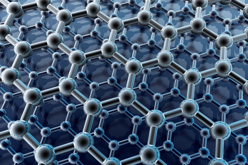
Graphene already has impressive properties: its sheets, made of single layers of carbon atoms arranged in hexagons, are stronger than steel and conduct electricity better than copper. It has shown superconductivity before3, but it occurred when in contact with other materials, and the behaviour could be explained by conventional superconductivity.
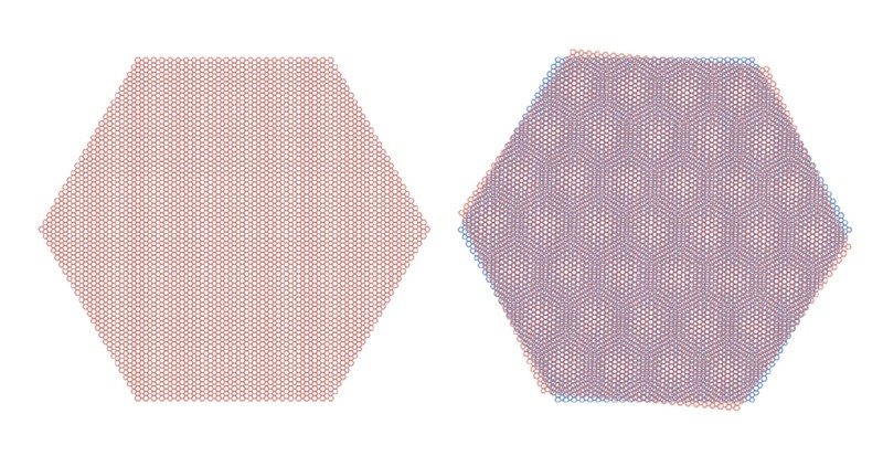
Physicist Pablo Jarillo-Herrero at the Massachusetts Institute of Technology (MIT) in Cambridge and his team weren’t looking for superconductivity when they set up their experiment. Instead, they were exploring how the orientation dubbed the magic angle might affect graphene. Theorists have predicted that offsetting the atoms between layers of 2D materials at this particular angle might induce the electrons that zip through the sheets to interact in interesting ways — although they didn’t know exactly how.
The team immediately saw unexpected behaviour in their two-sheet set-up. First, measurements of graphene’s conductivity and the density of the particles that carry charge inside it suggested that the construction had become a Mott insulator2 — a material that has all the ingredients to conduct electrons, but in which interactions between the particles stop them from flowing. Next, the researchers applied a small electric field to feed just a few extra charge carriers into the system, and it became a superconductor1. The finding held up in experiment after experiment, says Jarillo-Herrero. “We have produced all of this in different devices and measured it with collaborators. This is something in which we’re very confident,” he says.
A material made up of two layers of graphene, twisted at an angle of 1.1º (illustrated, right), show superconducting properties.Courtesy of the researchers
The existence of an insulating state so close to superconductivity is a hallmark of unconventional superconductors such as cuprates. When the researchers plotted phase diagrams that charted the material’s electron density against its temperature, they saw patterns very similar to those seen for cuprates. That provides further evidence that the materials may share a superconducting mechanism, says Jarillo-Herrero.
Finally, although graphene shows superconductivity at a very low temperature, it does so with just one-ten-thousandth of the electron density of conventional superconductors that gain the ability at the same temperature. In conventional superconductors, the phenomenon is thought to arise when vibrations allow electrons to form pairs, which stabilize their path and allow them to flow without resistance. But with so few available electrons in graphene, the fact that they can somehow pair up suggests that the interaction at play in this system should be much stronger than what happens in conventional superconductors.
Conductivity confusion
Physicists disagree wildly on how electrons might interact in unconventional superconductors. “One of the bottlenecks of high-temperature superconductivity has been the fact that we don’t understand, even now, what’s really gluing the electrons into pairs,” says Robinson.
But graphene-based devices will be easier to study than cuprates, which makes them useful platforms for exploring superconductivity, says Bascones. For example, to explore the root of superconductivity in cuprates, physicists often need to subject the materials to extreme magnetic fields. And ‘tuning’ them to explore their different behaviours means growing and studying reams of different samples; with graphene, physicists can achieve the same results by simply tweaking an electric field.
Kamran Behnia, a physicist at the Higher Institute of Industrial Physics and Chemistry in Paris, is not yet convinced that the MIT team can definitively claim to have seen the Mott insulator state, although he says the findings do suggest that graphene is a superconductor, and potentially an unusual one.
Physicists cannot yet state with certainty that the superconducting mechanism in the two materials is the same. And Laughlin adds that it is not yet clear that all the behaviour seen in cuprates is happening in graphene. “But enough of the behaviours are present in these new experiments to give cause for cautious celebration,” he says.
Physicists have been “stumbling around in the dark for 30 years” trying to understand cuprates, says Laughlin. “Many of us think that a light just switched on.”
While graphene has faced challenges in the field of digital logic because of its lack of an inherent band gap, it has been that very weakness that has attracted many researchers to exploring its use in optoelectronics. This lack of a band gap makes graphene an extreme broadband absorber, enabling photodetection for visible, infrared, and terahertz frequencies. (from spectrum.ieee.org )
Now, in research supported by the European Commission’s €1 billion ($1.3 billion) 10-year project, the Graphene Flagship, a group of universities—including the University of Cambridge in the UK, The Hebrew University in Israel, and John Hopkins University in the United States—has successfully combined graphene with silicon on a chip to make “high-responsivity” Schottky barrier photodetectors.
Such photodetectors are formed by a junction between metal and a semiconductor. Since photodetectors are a key building block of optoelectronic links, the result of this research could lead to far less energy being consumed to process and move information, a key achievement in realizing the potential of the Internet of Things (IoT), say the researchers.
In research described in the journal Nano Letters, these graphene-based photodetectors achieve a responsivity of 0.37 ampere of current per Watt of incident light on the photodiode using 1.55 micrometer light. This high responsivity is comparable to that of the silicon germanium detectors currently used in silicon photonics.
While silicon-based photodetectors can do the job for detecting visible light, they fall short when it comes to detecting near-infrared radiation (NIR). The reason for this is that the energy of NIR photons at telecom wavelengths is not strong enough to bridge the band gap of silicon. For this reason, photodetectors have been fashioned out of a combination of silicon and germanium, which requires a complex and comparatively expensive fabrication process. This new graphene-silicon combination could be far simpler and cheaper to produce.
“This is a significant result which proves that graphene can compete with the current state of the art by producing devices that can be made more simply, cheaply and work at different wavelengths,” said Andrea Ferrari, a professor at the University of Cambridge’s Graphene Center, in a press release. “Thus paving the way for graphene integrated silicon photonics.”
As far as achieving the aim of consuming less energy, Ferrari sees this most recent work as a significant achievement. “Graphene can beat current silicon photonic technology in terms of energy consumption,” he said.
Regarding optical communications for IoT: “This is a first step towards this, and, over the next two years the aim of the wafer-scale integration and optoelectronics work-packages of the Flagship is to really make this happen,” the University of Cambridge’s Ilya Goykhman said in a press release.
Over the next two years, this line of research will branch out from the photodetector that they have produced here to optical modulators.
Ferrari added: “We have shown the potential for the detector but we also need to produce a graphene-based modulator to have a full, low energy optical telecommunication system, and the Flagship is working hard on this problem.”
The use of graphene as a transparent conducting film has been hotly pursued of late, in large part because it offers a potentially cheaper alternative to indium tin oxide (ITO) where a bottleneck of supply seems to be looming. (from spectrum.ieee.org)
It has not been clear whether photovoltaic manufacturers have taken any interest in graphene as an alternative for transparent conducting films. This lack of interest may in part be the result of there being little research into whether graphene maintains its attractive characteristic of high carrier mobility when used in conjunction with silicon.
Now researchers at the Helmholtz Zentrum Berlin (HZB) Institute in Germany have shown that graphene does not lose its impressive conductivity characteristics even when mated with silicon.
“We examined how graphene’s conductive properties change if it is incorporated into a stack of layers similar to a silicon based thin film solar cell and were surprised to find that these properties actually change very little,” said Marc Gluba of the HZB Institute for Silicon Photovoltaics in a press release.
The research, which was published in the journal Applied Physics Letters (“Embedded graphene for large-area silicon-based devices”), used the method of growing the graphene by chemical vapor deposition on a copper sheet and then transferring it to a glass substrate. This was then covered with a thin film of silicon.
The researchers experimented with two different forms of silicon commonly used in thin-film technologies: amorphous silicon and polycrystalline silicon. In both cases, despite completely different morphology of the silicon, the graphene was still detectable.
“That’s something we didn’t expect to find, but our results demonstrate that graphene remains graphene even if it is coated with silicon,” said Norbert Nickel, another researcher on the project, in a press release.
In their measurements, the researchers determined that the carrier mobility of the graphene layer was roughly 30 times greater than that of conventional zinc oxide-based contact layers.
Although the researchers concede that connecting the graphene-based contact layer to external contacts is difficult, it has garnered the interest of their thin-film technology colleagues. “Our thin film technology colleagues are already pricking up their ears and wanting to incorporate it,” Nickel adds.